Contact: Matthew Yankowitz
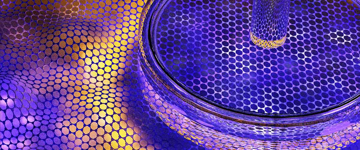
TALLAHASSEE, Fla. — An international team of researchers working at the National MagLab has developed a technique to manipulate the electrical conductivity of graphene with compression, bringing the material one step closer to being a viable semiconductor for use in today's electronic devices.

Matthew Yankowitz, a postdoc in Cory Dean's group at Columbia University, is the lead author on the study.
"Graphene is the best electrical conductor that we know of on Earth," said Matthew Yankowitz, a postdoctoral research scientist in Columbia University's physics department and first author on the study. "The problem is that it's too good at conducting electricity, and we don't know how to stop it effectively. Our work establishes for the first time a route to realizing a technologically relevant band gap in graphene without compromising its quality. Additionally, if applied to other interesting combinations of 2D materials, the technique we used may lead to new emergent phenomena, such as magnetism, superconductivity, and more."
The study, funded by the National Science Foundation and the David and Lucille Packard Foundation, appears in the May 17 issue of Nature.
The unusual electronic properties of graphene, a two-dimensional (2D) material comprised of hexagonally-bonded carbon atoms, have excited the physics community since its discovery more than a decade ago. Graphene is the strongest, thinnest material known to exist. It also happens to be a superior conductor of electricity — the unique atomic arrangement of the carbon atoms in graphene allows its electrons to easily travel at extremely high velocity without the significant chance of scattering, saving precious energy typically lost in other conductors.
But turning off the transmission of electrons through the material without altering or sacrificing the favorable qualities of graphene has proven unsuccessful to-date.

Cory Dean at the MagLab.
"One of the grand goals in graphene research is to figure out a way to keep all the good things about graphene but also create a band gap – an electrical on-off switch," said Cory Dean, assistant professor of physics at Columbia University and the study's principal investigator. He explained that past efforts to modify graphene to create such a band gap have degraded the intrinsically good properties of graphene, rendering it much less useful. One superstructure does show promise, however. When graphene is sandwiched between layers of boron nitride (BN), an atomically-thin electrical insulator, and the two materials are rotationally aligned, the BN has been shown to modify the electronic structure of the graphene, creating a band gap that allows the material to behave as a semiconductor — that is, both as an electrical conductor and an insulator. The band gap created by this layering alone, however, is not large enough to be useful in the operation of electrical transistor devices at room temperature.
In an effort to enhance this band gap, Yankowitz, Dean, and their colleagues at the National MagLab, the University of Seoul in Korea, and the National University of Singapore, compressed the layers of the BN-graphene structure and found that applying pressure substantially increased the size of the band gap, more effectively blocking the flow of electricity through the graphene. MagLab physicist David Graf and team worked with Columbia to develop the capability to integrate electrical measurements of these devices under high pressure and at cryogenic temperatures in the presence of high magnetic fields at the MagLab's DC Field Facility.
"The work of Yankowitz and co-workers is a great example of users and MagLab staff collaborating to explore quantum matter by coupling graphene's unique properties with the thermodynamic tuning parameters of high pressure and high magnetic fields," said DC Field Director Tim Murphy. "The result is the ability to dynamically influence the band structure of these materials and explore the resulting quantum states."
"As we squeeze and apply pressure, the band gap grows," Yankowitz explained. "It's still not a big enough gap — a strong enough switch — to be used in transistor devices at room temperature, but we have gained a fundamentally better understanding of why this band gap exists in the first place, how it can be tuned, and how we may target it in the future. Transistors are ubiquitous in our modern electronic devices, so if we can find a way to use graphene as a transistor it would have widespread applications."
Yankowitz added that scientists have been conducting experiments at high pressures in conventional three-dimensional materials for years, but no one had yet figured out a way to do them with 2D materials. Now, researchers will be able to test how applying various degrees of pressure changes the properties of a vast range of combinations of stacked 2D materials.
"Any emergent property that results from the combination of 2D materials should grow stronger as the materials are compressed," Yankowitz said. "We can take any of these arbitrary structures now and squeeze them and the strength of the resulting effect is tunable. We've added a new experimental tool to the toolbox we use to manipulate 2D materials and that tool opens boundless possibilities for creating devices with designer properties."
Story courtesy of Columbia University


